Japan’s New Semiconductor Offensive
Japan Bets on Rapidus in Chips Race: An Interview with Nishikawa Kazumi (Part 2)
Economy Politics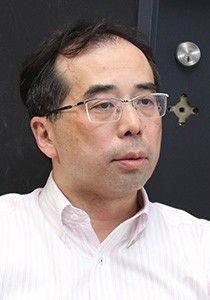
Nishikawa Kazumi
Senior Director of Ministry of Economy, Trade, and Industry’s Trade and Economic Security Bureau. Born in Osaka Prefecture in 1973. Graduated from the University of Tokyo and joined METI (then the Ministry of International Trade and Industry) in 1996. Headed the Policy Planning and Coordination Division of the Commerce and Information Policy Bureau, the Economic Security Office, and was Counselor to the Minister of Economy, Trade, and Industry’s Secretariat before assuming his current post.
- English
- 日本語
- 简体字
- 繁體字
- Français
- Español
- العربية
- Русский
(Continued from part 1.)
METI and the Race for Next-Generation Semiconductors
TAKENAKA HARUKATA Rapidus Corporation was launched in August 2022 with funding by a consortium of eight major Japanese companies. The following November, the business announced a partnership with IBM to commercialize emerging 2-nanometer semiconductor technology. Then in December, it signed a memorandum of cooperation with Europe’s Interuniversity Microelectronics Centre, or Imec. The goal is to begin production in 2027. Can you give us some background on how Rapidus was formed?
NISHIKAWA KAZUMI Development of the next generation of semiconductor technologies has been high on the agenda since 2020. There are two basic components here. One is the development of GAA, or “gate-all-around,” transistor technology to replace FinFET. The other is advanced back-end packaging technology. We took on both of these challenges in the spring of 2021 by launching a major R&D program headquartered in Tsukuba, at the National Institute of Advanced Industrial Science and Technology, or AIST. In respect to the first goal, we’ve budgeted about 42 billion yen to finance a research project that brings together semiconductor experts from Japanese makers like Canon and Tokyo Electron and foreign firms like Samsung and Intel to develop foundational 2-nanometer technology. With regard to the second goal, in February 2021, Taiwan Semiconductor Manufacturing Co. announced plans for its Japan 3DIC R&D Center, which is currently operating in Tsukuba as well.
Going back much further, semiconductor researchers from American and Japanese companies, including IBM and Tokyo Electron, began working together in Albany, New York, some twenty years ago to develop new circuit-miniaturization technology, and the result was IBM’s prototype 2-nanometer chip using GAA transistor architecture announced in May 2021. I call it IBM’s prototype, but it was actually the product of collaboration between Japanese and US companies.
Not long ago, IBM asked for help putting this prototype into high-volume production. Rapidus was founded for that purpose under the leadership of President Koike Atsuyoshi and Chairman Higashi Tetsurō.
Is Rapidus METI’s Creation?
TAKENAKA When the Ministry of Economy, Trade, and Industry released its initial Strategy for Semiconductors and the Digital Industry in June 2021, there was no mention of collaboration with US industry, but the idea figures prominently in the revised plan released in November 2021. One gets the feeling some fairly concrete agreement must have been reached in the interim, whether between METI and the US Department of Commerce or between Rapidus’s Koike and IBM. Is that an accurate understanding?
NISHIKAWA Well, yes and no. In terms of government policy, the June 2021 strategy had already targeted the two challenges I mentioned above, and work on those was underway in Tsukuba. Of course, inasmuch as this is foundational technology, we were also discussing the need for further Japan-US collaboration. I remember discussing that in November 2021—that Japan couldn’t do it alone, that we needed to work in partnership with major Western research centers like Imec. But we weren’t talking about forming a private company. As for IBM’s initial approach, you would be better off asking Chairman Higashi or President Koike about that.
TAKENAKA So, what role did METI play in the establishment of Rapidus?
NISHIKAWA Higashi Tetsurō, who assumed the post of chairman of Rapidus in August 2022, was also the chair of the panel that drafted the Semiconductor and Digital Industry Strategy. It’s true that he spoke a good deal about the importance of 2-nanometer technology. But the leadership of Higashi and Koike was the impetus behind the creation of Rapidus.
If you think something is important, you have to be willing to take the lead yourself, or no one else is going to get on board. In the past, the government might have brought together companies involved in a particular field, having them provide the funding and personnel needed to embark on some new project—which sometimes wasn’t even clearly defined until the bureaucracy assembled the engineers and discussed what would be done. Rapidus represents a completely different approach. Two men, the core figures, decided to form Rapidus, and they personally approached the eight participating companies. It’s true that METI was consulted, and the ministry has provided a lot of support because it wants the venture to succeed. But whoever wrote that METI created Rapidus has got their facts wrong.
TAKENAKA Still, I think there’s a pretty widespread perception that Rapidus is a government-sponsored business and that METI was deeply involved in its founding.
NISHIKAWA METI has assisted with the financial side of things, and it’s made it easier for companies to invest in Rapidus by communicating the importance that the ministry places on this field. But the company would never have been established if it weren’t for Higashi and Koike.

METI official Nishikawa Kazumi (left) with interviewer Takenaka Harukata, chair of the Nippon.com Editorial Planning Committee. (© Nippon.com)
Targeting Low-Volume Specialty Chips
TAKENAKA Rapidus has said that its purpose is to build Japan’s capacity to manufacture and sell cutting-edge logic semiconductors. But a lot of people seem skeptical about that goal. Big foundries like TSMC are already at work on mass-production of 2-nanometer chips. And it’s said that the big tech companies have begun designing their own specialty semiconductors in-house. What segment is Rapidus targeting?
NISHIKAWA As Koike explains it, they’re focusing on specialty semiconductors at relatively low volumes. If you’re talking about semiconductors for smartphones, Apple sells upwards of 200 million iPhones a year, so that means it needs the same number of advanced microprocessors. That’s why a firm like Apple can afford to spend huge sums designing its own semiconductors.
On the other hand, if a company like Toyota or Volkswagen wants state-of-the-art semiconductors for its high-end self-driving vehicles, it’s not going to need more than a few hundred thousand chips. With that level of demand, it doesn’t make sense for a company to spend all those resources on in-house chip design.
Rapidus aims to devise ways of designing state-of-the-art conductors more cheaply and delivering them faster. There are two basic ways to approach the challenge. One is chiplet technology. This involves manufacturing tiny integrated circuits with specific functionalities that can be bonded together afterward to create a single chip. Connecting them sounds easy, but it’s quite difficult; it will hinge on the development of advanced packaging technology. Another approach might involve the use of AI. Here the focus would be on how much you can reduce the cost and time needed for chip design by using generative AI to design the circuits.
High Price Tags Attached
TAKENAKA A huge amount of government funding has already been channeled into Rapidus.
NISHIKAWA The supplementary budget passed at the end of 2021 included 110 billion yen for R&D, and 70 billion yen of that was awarded to Rapidus in November 2022. More recently, the government awarded the company an additional 260 billion yen from the 450 billion yen allocated for R&D in the fiscal 2022 supplementary budget. The rest of that 450 billion yen is being used for other things, such as development of next-generation memory and optoelectronic technology.
These budget allocations aren’t intended to fund the whole development process up front. We’re using the stage-gate funding model, evaluating progress at each stage before proceeding to the next phase of funding. There were three “gates” for the initial 70 billion-yen phase. The first was whether the company could secure licensing for the chip prototype at a reasonable cost, including know-how. The second related to the lithographic equipment needed to develop an advanced extreme ultraviolet production process—whether they could secure the cooperation of Imec and the Dutch manufacturer ASML, which produces the lithography equipment. The third gate was a concrete plan for construction of a pilot production line.
TAKENAKA Some people with technical expertise in this area have argued that it’s unrealistic for Japan, which currently has nothing more advanced than 40-nanometer technology, to jump from there to manufacture of 2-nanometer chips. How do you respond to those critics?
NISHIKAWA It wouldn’t be realistic if we were starting from square one, but as I noted, Japanese and American companies have been working together for twenty years to produce the 2-nanometer prototype. If we use that technology, Rapidus can compress the development time by quite a bit. And by securing the cooperation of Imec and ASML as well, they think they can put the plan on a realistic footing.
TAKENAKA Last February, Rapidus announced that it had chosen Chitose in Hokkaidō as the site for its semiconductor plant. That’s not an area where the industry has any presence to speak of. Was METI involved in choosing the location?
NISHIKAWA The ministry was consulted on this and that, but the final decision was Rapidus’s alone. As I understand it, the biggest deciding factor was the availability of a large enough construction site. We’re talking about 100 hectares, and preparing such a site from scratch would take too long. There weren’t that many candidates.
For an operation on this scale, moving into an area where semiconductor fabs are already operating would not be helpful in terms of securing personnel. They’re going to have to bring in engineers at the start, and from a long-term perspective, they’ll need to work with local universities and colleges of technology to develop human resources.
TAKENAKA We’re told that Rapidus will need trillions more in R&D funding over the next few years. Is the government prepared to continue subsidizing the business?
NISHIKAWA When you’re undertaking a mammoth R&D project that entails substantial risk, the state has a role to play in supporting the undertaking. But the whole process has to be monitored and funded carefully, using the sort of stage-gate mechanism I mentioned. As the company gets closer to high-volume production, it will obviously need to rely more on financing from the private sector. At that point, the challenge will be securing major injections of funds when they’re needed.
Japan as a Smart Tech Investment
TAKENAKA This past June, METI revised its Strategy for Semiconductors and the Digital Industry. Can you take us through the key changes in that basic policy document?
NISHIKAWA The new strategy sets a clear 2030 sales target of 15 trillion yen. Also, in addition to logic chips, it covers memory and power semiconductors, image sensors, and advanced packaging technology.
In addition, there’s an awareness that AI will be playing an increasingly important role from here on. Japan needs to incorporate that enhanced computing power in its industrial base. We need to establish our own industrial base where AI is concerned, but in addition to that, we need to understand that generative AI is bound to trigger an explosion in demand for the kind of advanced semiconductors targeted by companies like TSMC and Rapidus.
TAKENAKA On May 18, Prime Minister Kishida Fumio held an exchange of views with the senior executives of seven global semiconductor companies, including the US firms Intel, Micron, and IBM; South Korea’s Samsung; and Taiwan’s TSMC. What was the significance of this meeting, in your view?
NISHIKAWA The executives at the meeting were from businesses that had already committed themselves, to one degree or another, to large-scale investments in Japan and its semiconductor industry. The purpose was to discuss Japan’s future place in global semiconductor supply chains.
Japan has begun to attract a lot of interest from abroad over the past two years. In November 2021, shortly after Kishida took office, the Japanese government allocated 61.7 billion yen to encourage investment by advanced chipmakers. Of course, another economic inducement, of which we’re not very proud, is the fact that labor and other costs here have fallen, relatively speaking. More importantly, though, Japan has first-rate construction companies like Kajima, which is doing such a great job in Kumamoto. As word gets around that work on the TSMC plant is proceeding smoothly and on schedule, other companies are going to take a closer look at Japan. And when they hear the news that Kishida has met with people like AI pioneer Sam Altman, they’ll begin to realize that things are really moving here, and that Japanese-made semiconductors could be a smart investment.
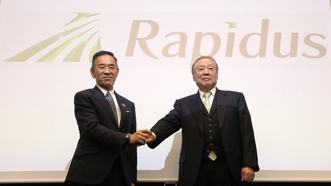
(Originally written in Japanese by Ishii Masato of the Nippon.com Editorial Department based on a June 22, 2023, interview. Banner photo: Rapidus President Koike Atsuyoshi, at left, and Chairman Higashi Tetsurō at a press conference in Tokyo on November 11, 2022. © Jiji.)